Table of Contents >> Show >> Hide
- What Is Pad Printing?
- Why Artistic PCBs Need More Color
- How Pad Printing Changes PCB Art
- Choosing the Right PCB Surface
- Ink Selection for Pad Printing on PCBs
- Designing Artwork for Pad Printing
- Pad Printing Before or After Assembly?
- Multi-Color Pad Printing for PCBs
- Common Problems and Fixes
- When Pad Printing Makes Sense
- Practical Example: A Two-Color Badge
- Experiences and Lessons From Using Pad Printers To Add Color To Artistic PCBs
- Conclusion
- SEO Tags
For decades, printed circuit boards were expected to do one job: behave. They carried current, held components, survived heat, and hid inside beige boxes like tiny green accountants. Then makers, badge designers, hardware artists, and open-source electronics fans looked at those fiberglass rectangles and asked a dangerous question: “What if the circuit board could also be the artwork?”
That question gave us artistic PCBs: boards where copper pours become shading, solder mask becomes background color, silkscreen becomes illustration, and LEDs become punctuation marks. The problem is that the traditional PCB color palette is limited. A typical board gives you substrate, copper finish, one solder mask color, and one silkscreen color. That is enough for labels and logos, but not enough for a designer who wants orange flames, blue waves, red lips, or a tiny robot wearing shoes that absolutely did not pass electrical safety review.
This is where pad printing enters the workshop like a quiet wizard with an ink cup. Pad printing can add spot colors to finished PCBs, making it possible to create richer, more expressive boards without redesigning the entire fabrication process. It is not magic, although after the first clean print lands perfectly on a glossy solder mask, it can feel suspiciously close.
What Is Pad Printing?
Pad printing is an indirect printing method that transfers ink from an etched plate, often called a cliché, to a surface using a flexible silicone pad. The etched plate holds the image. The ink fills the etched area. The silicone pad picks up the ink and presses it onto the target object. Because the pad is soft and adaptable, it can print on surfaces that are flat, curved, textured, recessed, or awkwardly shaped.
That flexibility is why pad printing is used on objects such as pens, medical devices, toy parts, electronic enclosures, buttons, appliance panels, watch faces, and promotional products. The same feature also makes it surprisingly useful for artistic printed circuit boards. PCBs are flat enough to register accurately, but their surfaces may include solder mask, exposed metal pads, vias, routed edges, component outlines, and small height changes. A silicone pad can handle those better than many rigid printing approaches.
The Basic Pad Printing Workflow
A typical pad printing cycle looks like this:
- The artwork is etched into a cliché.
- Ink floods the etched area.
- A doctor blade or sealed ink cup removes extra ink from the plate surface.
- The solvent in the exposed ink film begins to evaporate, making the ink tacky.
- The silicone pad presses onto the cliché and picks up the image.
- The pad moves to the PCB and presses the image onto the board.
- The ink dries or cures, depending on the ink system.
In plain English: it is a very precise rubber stamp, except the stamp is made of silicone, the design comes from an etched plate, and the ink chemistry matters enough to make your casual hobby project feel like a tiny industrial science fair.
Why Artistic PCBs Need More Color
Standard PCB fabrication already provides a few visual layers. The fiberglass core is usually pale yellow or tan. Copper can appear reddish before finishing, or silver/gold after surface finish. Solder mask provides the dominant board color. Silkscreen adds text, reference designators, polarity marks, logos, and sometimes decorative art.
But every one of those layers has limits. Solder mask is usually one color per side. Silkscreen is typically one color, most often white or black. Some manufacturers offer colored silkscreen or full-color UV printing, but availability, cost, heat resistance, finish, and minimum order quantities vary. For mass-produced artistic badges or limited-run collectible boards, designers often want one or two extra colors without committing to an expensive specialty process.
Pad printing solves a specific problem: it lets you add small, controlled areas of color after the PCB has been fabricated. That means your base board can still be manufactured by a normal PCB house, while the decorative layer can be handled as a secondary operation.
How Pad Printing Changes PCB Art
PCB art is usually built from constraints. Designers use copper, solder mask openings, exposed finish, silkscreen, routed shapes, castellations, LEDs, and component placement to create visual effects. That constraint-based approach is part of the charm. However, pad printing adds a new layer of creative freedom: independent color.
Instead of choosing between a blue solder mask or a red solder mask, a designer can use a black solder mask, white silkscreen, and then pad print red accents. Or the board can use white solder mask as a canvas, black silkscreen for linework, and orange pad printing for highlights. On a badge shaped like a flame, orange pad printing is not just decoration; it is the difference between “nice circuit board” and “this thing looks like it escaped from a cyberpunk campfire.”
Spot Color Is the Sweet Spot
Pad printing is especially good for spot colors: logos, icons, character details, colored stripes, warning marks, decorative fills, and limited graphic accents. It is less ideal for covering an entire board with a perfect full-color photograph. For that, UV printing or other digital processes may be better. But for bold artwork, themed badges, product branding, and small production runs, pad printing can be practical, affordable, and visually striking.
Choosing the Right PCB Surface
The surface of the PCB matters. Ink adhesion depends on solder mask type, gloss level, cleanliness, surface energy, and curing conditions. Glossy solder masks can look beautiful but may be harder for some inks to grip. Matte solder masks may provide a friendlier surface but can change the look of the final color. White solder mask makes colors pop, while black solder mask can create dramatic contrast but may require more opaque inks.
Before printing a production batch, test the exact board finish. A pad print that works beautifully on a spare green prototype may behave differently on a matte black production panel. PCBs are not blank paper; they are engineered laminates with coatings, plating, and residues that can affect adhesion.
Cleanliness Is Not Optional
Boards should be clean before printing. Fingerprints, flux residue, dust, packaging oils, silicone contamination, and random workshop crumbs can ruin adhesion. A clean board gives the ink a fighting chance. A dirty board turns the print into abstract art, usually not the profitable kind.
For serious work, use a controlled cleaning process approved for the solder mask and final finish. Avoid aggressive solvents unless you know they will not damage the board. If adhesion is still weak, surface treatment such as plasma or corona treatment may help improve wetting, but it should be tested carefully because PCBs include multiple materials and exposed conductive features.
Ink Selection for Pad Printing on PCBs
The ink must match the job. For artistic PCBs, the ideal ink is opaque, durable, compatible with the solder mask, and resistant to handling. If the board will be assembled after printing, the ink must also survive the assembly process. That can include reflow temperatures, cleaning chemistry, abrasion, packaging, and years of being poked by proud owners who say, “Look, it blinks.”
Two-component epoxy or industrial pad printing inks are often considered for durable applications because they cure into tougher films than simple decorative inks. UV-curable inks can work in some workflows, but heat stability must be verified. Some decorative UV inkjet prints may not tolerate a standard reflow oven, which is why pad printing with temperature-stable inks remains interesting for hardware artists.
Drying vs. Curing
Drying and curing are not the same thing. Drying usually means solvent leaves the ink film and the print becomes dry to the touch. Curing means the ink reaches its intended chemical and mechanical performance. A print may feel dry in minutes but still need hours or days to fully cure. Testing too early can make a good ink look bad. Patience is not glamorous, but neither is explaining why every badge in your batch has a blue thumbprint.
Designing Artwork for Pad Printing
Good pad printing starts before the machine is turned on. The artwork should be designed with the process in mind. Thin lines, tiny text, halftones, and large solid fields all behave differently. The cliché depth, ink viscosity, pad shape, pressure, and board surface determine whether the printed result looks crisp or resembles a tired jellyfish.
For PCB artwork, begin with vector graphics. Keep registration marks outside the final visible area or use board features such as tooling holes, routed corners, or panel rails for alignment. If the board will receive more than one pad-printed color, each color needs its own plate and setup. Registration between colors must be considered from the beginning, not after the first 300 boards are printed slightly cross-eyed.
Design Rules That Actually Help
- Use bold shapes for the first experiments.
- Avoid placing ink over solder pads, test points, connectors, or exposed contacts.
- Leave clearance around components if printing after assembly.
- Use high-contrast color combinations for readability.
- Test ink opacity on the actual solder mask color.
- Use panelized boards when possible to improve handling and alignment.
- Build a few sacrificial boards into the run for setup and test prints.
The best early project is not a full-color Renaissance painting on a USB badge. Start with a logo, symbol, stripe, or highlight. Learn how the ink behaves. Then become dangerous.
Pad Printing Before or After Assembly?
One of the biggest workflow questions is whether to pad print before or after PCB assembly. Both options have advantages.
Printing before assembly gives you a flat board surface, easier fixturing, and fewer obstacles. It also reduces the risk of hitting components with the pad. However, the printed ink must survive solder paste application, pick-and-place handling, reflow heat, cleaning, and inspection.
Printing after assembly avoids exposing the artwork to reflow, but it introduces new challenges. Components create height differences. The pad may contact tall parts. Ink must not contaminate connectors, switches, sensors, or LEDs. Fixturing becomes more complex. For simple decorative areas away from components, post-assembly printing can work. For dense boards, it may become a mechanical comedy routine with expensive consequences.
For many artistic PCB projects, printing before assembly is the cleaner route, provided the ink is tested for heat resistance. For purely decorative collectibles that will not go through reflow after printing, post-fabrication and pre-packaging printing may be ideal.
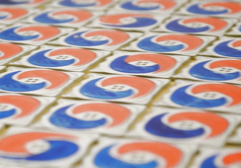
Multi-Color Pad Printing for PCBs
Multi-color pad printing is possible, but each color adds complexity. A two-color design needs two plates, two ink setups, and accurate registration. If the colors overlap, trapping and print order matter. If they sit side by side, alignment matters even more because the human eye is very good at noticing tiny mistakes, especially after you have proudly announced the board as “limited edition.”
For artistic PCBs, two strong spot colors can have more impact than four fussy colors. For example, a black solder mask board with white silkscreen and red pad-printed highlights can look premium. A white solder mask board with blue and orange pad printing can look playful and modern. A purple solder mask board with metallic gold print can look like royalty joined a hackerspace.
Registration Tips
Accurate registration depends on stable fixturing. The board should sit in the same position every time, ideally using tooling holes, panel rails, edge stops, or a custom nest. If the board shifts, the print shifts. If the print shifts, the artwork becomes “experimental.” That word is useful in galleries, less useful when customers paid for clean graphics.
Use test prints on scrap boards or transparent film to tune alignment. Keep the setup notes. Record pad type, ink mix, thinner ratio, pressure, dwell time, plate details, cure schedule, and room conditions. Future you will thank present you. Future you is usually tired.
Common Problems and Fixes
Ink Does Not Stick
Possible causes include contamination, low surface energy, incompatible ink, insufficient cure, or the wrong thinner. Clean the board, test surface treatment, verify ink compatibility, and allow full cure before adhesion testing.
Print Looks Blurry
Blurry prints can come from too much pad pressure, excessive ink, poor cliché quality, board movement, or a pad that is too soft. Reduce pressure, improve fixturing, adjust ink viscosity, or try a different pad shape.
Color Looks Weak
Low opacity is common when printing light colors on dark solder mask. Use high-opacity ink, adjust print thickness, consider a white underprint, or redesign the artwork so the base PCB color supports the final look.
Ink Smears During Handling
The print may be dry but not cured. Extend cure time, add heat if recommended by the ink supplier, and avoid stacking boards too soon. A rack is cheaper than a ruined batch.
When Pad Printing Makes Sense
Pad printing is a strong option when the design needs limited extra color, repeatability, and a professional finish. It is especially attractive for conference badges, collectible add-ons, boutique electronics, custom keyboard PCBs, art boards, limited-edition developer kits, branded hardware, and product panels where the PCB itself is visible.
It may not be the best choice for one-off full-color images, extremely large graphics, or designs that require photographic gradients. It also may not make sense if your PCB manufacturer already offers affordable full-color printing that meets your durability and heat requirements. The right method depends on the design, budget, production volume, and assembly process.
Practical Example: A Two-Color Badge
Imagine a small conference badge shaped like a retro rocket. The PCB uses matte black solder mask. White silkscreen creates stars, labels, and outlines. Exposed ENIG pads add gold details for windows and connector accents. The designer wants orange flames and blue exhaust because rockets without color are just office supplies with ambition.
The base PCB is fabricated normally. The orange flame artwork is etched into one cliché, and the blue exhaust artwork is etched into another. The boards are held in a custom fixture using panel tooling holes. Orange prints first, cures partially, then blue prints second. After full cure, adhesion is tested with tape, light abrasion, and a reflow simulation if assembly will happen afterward. Once the ink passes, the batch moves to assembly.
The result is still a real circuit board, but it now has visual energy. The electronics work, the art reads instantly, and the badge stands out on a crowded lanyard. That is the point of artistic PCBs: function and personality sharing the same fiberglass apartment.
Experiences and Lessons From Using Pad Printers To Add Color To Artistic PCBs
The first experience most people have with pad printing PCBs is humility. On paper, the process sounds simple: make a plate, add ink, press pad, admire masterpiece. In reality, the first few attempts often teach you that ink has opinions. It may cling to the cliché, split on the pad, refuse to release, dry too quickly, smear at the edge, or print beautifully once and then act like it has joined a labor union.
One useful lesson is to treat the board as both an electronic part and an art substrate. In normal PCB design, you might worry about trace width, solder mask expansion, drill tolerance, and component clearance. With pad printing, you add a second set of concerns: surface cleanliness, ink opacity, print pressure, registration, cure time, and handling. The two worlds overlap. For example, an exposed test pad might be electrically convenient but visually distracting. A gorgeous printed stripe might accidentally cross a programming header. Good artistic PCB work requires both the engineer and the designer in your brain to stop arguing and share snacks.
Another lesson is that fixtures are worth more than heroic hand alignment. A simple acrylic, aluminum, or 3D-printed nest can save hours. If the board has tooling holes, use them. If it has a panel rail, use it. If it has a distinctive routed outline, build stops around it. The more repeatable the placement, the less you have to rely on luck. Luck is not a process control strategy, although it has appeared in many project postmortems under different names.
Color testing is also essential. A bright ink in the container may look completely different on black solder mask. Some colors need a white base layer to appear vivid. Metallic inks may look stunning but require extra testing for durability and compatibility. A color that looks perfect under desk lighting may shift under sunlight or event hall LEDs. If the PCB will be photographed, sold, worn, or displayed, view the samples under real conditions.
Handling discipline matters more than beginners expect. Freshly printed boards should not be stacked face-to-face. They should not be tossed into a box “just for a minute.” They should not be tested by every curious friend within reach. Use drying racks, gloves, labels, and a clear cure schedule. Document what worked. A notebook entry that says “blue print good, 15 percent thinner, medium pad, low pressure, cured overnight” can rescue a future production run.
The biggest creative lesson is that pad printing does not need to do everything. It shines when it adds the one color the PCB process cannot easily provide. Use copper for shine, solder mask for mood, silkscreen for line art, LEDs for drama, and pad printing for accents. When all layers work together, the board feels intentional rather than decorated. That is when an artistic PCB stops being a circuit with graphics and becomes a small manufactured object with personality.
Conclusion
Using pad printers to add color to artistic PCBs is a practical way to push circuit board design beyond the usual solder mask and silkscreen palette. It gives makers, badge designers, and boutique hardware creators a way to add spot colors, branding, highlights, and character without abandoning conventional PCB fabrication. The process does require testing, clean surfaces, compatible inks, careful curing, and repeatable fixturing. It is not a shortcut around craftsmanship; it is another tool for it.
For the right project, pad printing can turn a board from “nice prototype” into “wait, where did you get that?” It lets electronics wear color proudly. And in a world full of hidden circuit boards, artistic PCBs remind us that even functional objects deserve a little stage presence.