Table of Contents >> Show >> Hide
- Why Data Storage Still Isn’t “One Size Fits All”
- Phase-Change Memory: The “Crystal vs. Glass” Switch
- The “Seismic” Breakthrough: A Semiconductor That Shocks Itself
- Why This Could Be a Big Deal for Real Devices
- Where This Fits Among the “Next-Gen Memory” Contenders
- Reality Check: From Beautiful Physics to Boring, Wonderful Products
- What “Holy Grail” Could Look Like in Everyday Tech
- So, Is This the Future of Data Storage?
- Real-World “Experiences” From the Data-Storage Frontier (Extra )
- 1) The “Why Is My Laptop Fan Doing Its Best Jet Engine Impression?” Moment
- 2) The “My Phone Is at 12% and It’s 2 P.M.” Experience
- 3) The Gamer’s “Loading Screen: The Miniseries” Problem
- 4) The Data Engineer’s “Why Is My Database Waiting on I/O Again?” Headache
- 5) The Researcher’s “This Result Is Beautiful, Now Please Survive Reality” Rite of Passage
- Conclusion
If your laptop had a memory, it would be the kind that forgets everything the moment you sneeze on the power button.
That’s not a roastit’s basically how modern computing is built. We’ve spent decades living with a split personality:
fast memory that’s forgetful (RAM), and long-term storage that’s loyal but slower (flash/SSDs).
The “holy grail” is a single technology that can do bothfast, dense, durable, and nonvolatilewithout guzzling energy or
turning into a tiny space heater.
Now comes a discovery that sounds like science fiction and reads like a disaster movie:
a “weird” semiconductorindium selenide (In2Se3)that can flip its structure
from crystalline to glassy using shock-like effects triggered by electric current. Researchers describe the process
like an avalanche and an earthquake happening inside the material. The punchline?
It can do the crucial “crystal-to-glass” switch at dramatically lower power density than the conventional method.
If this scales into real devices, it could make phase-change memory far more practicaland bring “universal memory”
a lot closer to reality.
Why Data Storage Still Isn’t “One Size Fits All”
Computing today is a carefully choreographed relay race:
- CPU caches are lightning-fast but tiny.
- DRAM (your system RAM) is fast and roomybut volatile, meaning it loses data when power is off.
- NAND flash (SSDs/phone storage) remembers data without power, but writes are slower and more complex.
This is why your phone can store 50,000 photos but still stutter when you open five apps, a map, and a game at once.
RAM is your “right now” workspace; storage is your “keep this forever” closet. The gap between them is called the
memory wall, and it’s a major reason performance and energy efficiency don’t improve as fast as we’d like.
The dream is a memory that’s as fast as RAM, as persistent as storage, and
as energy-sipping as a sensible houseplant. That’s the “holy grail” people mean when they say
universal memory.
Phase-Change Memory: The “Crystal vs. Glass” Switch
Phase-change memory (PCM) is one of the most compelling contenders for universal memory because it stores information
in a surprisingly intuitive way: by switching a material between two structural states:
- Crystalline (ordered atoms) typically lower electrical resistance.
- Amorphous (disordered, glass-like atoms) typically higher electrical resistance.
If that sounds familiar, it should. Related phase-change materials have been used in rewritable optical media
(think CD/DVD technologies), where a laser toggles reflectivity by switching phases. In PCM chips, electrical signals
(instead of lasers) do the switching, and the device reads “0” or “1” by measuring resistance.
The Catch: Traditional Switching Is Hot (Literally)
The classic way to form the amorphous state is called melt–quench:
heat the material until it melts, then cool it fast so atoms “freeze” in a disordered arrangement.
It works, but it’s energy-hungry and can create tricky thermal engineering problemsespecially when you want
billions (or trillions) of cells packed tightly together.
That energy and heat burden is a big reason PCM hasn’t fully replaced DRAM or NAND at scale, even though it’s been
studied intensely and explored in commercial “storage-class” directions.
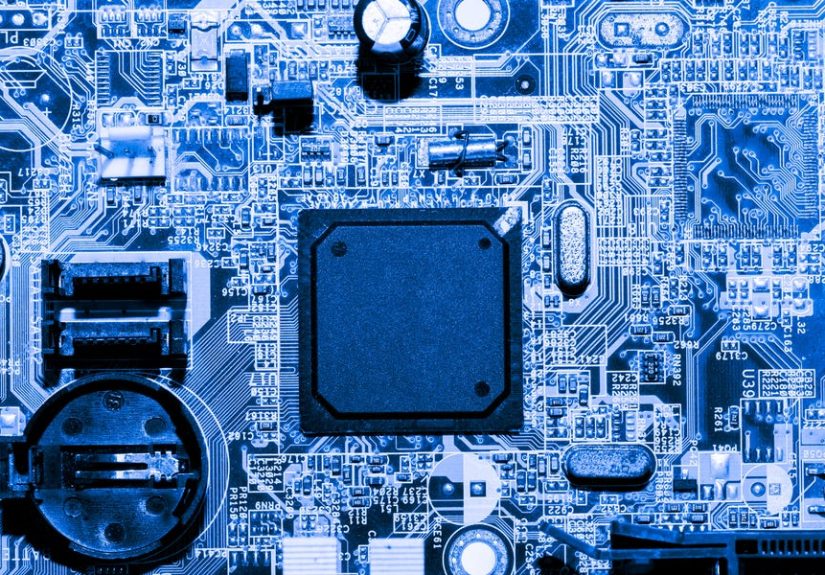
The “Seismic” Breakthrough: A Semiconductor That Shocks Itself
Researchers from Penn Engineering, collaborating with the Indian Institute of Science (IISc) and MIT, reported a new
way to amorphize indium selenide (In2Se3) nanowires using
direct currentnot the usual pulsed melting approach.
The headline-worthy claim is the ultralow power density needed for the transformation in this system,
described as up to a billion times lower than conventional melt–quench routes in this context.
This isn’t just “we made it a bit more efficient.” It’s “we found a different pathway to the same structural end state.”
And the pathway is bizarre in the best way.
Why In2Se3 Is Not Your Average Semiconductor
Indium selenide has a combination of properties that make it unusually responsive to electric fields and mechanical stress:
- Ferroelectricity: it can have a built-in electrical polarization.
- Piezoelectricity: mechanical stress can generate electrical effects, and electric fields can cause deformation.
- Layered/2D-like structure: parts of the crystal can “slip” relative to one another under the right conditions.
Think of it like a layered dessert where the middle layer can slide if you push it just rightexcept the dessert is a nanowire,
and the push is an electric current.
An Avalanche, an Earthquake, and a Microscopic “Acoustic Jerk”
Here’s the simplified picture of what the researchers observed:
-
Under a continuous current, tiny regions begin to deform and locally amorphize at the nanoscale.
The material’s layered structure and piezoelectric behavior help nudge parts of the lattice into unstable configurations. - Once a critical threshold is reached, deformation spreads rapidlylike an avalanche.
- The deformed regions collide and create a traveling mechanical disturbancean “acoustic jerk”similar in spirit to seismic waves.
- That disturbance helps link many small disordered regions into a much larger amorphous zone, extending to micrometer scales.
Translation: instead of “cook it and freeze it,” the material essentially “shifts, slips, and shock-waves” its way into a glassy state.
It’s a solid-state transformation driven by coupled electrical and mechanical effectsexactly the kind of physics that makes
materials scientists stare into space and whisper, “Wait… seriously?”
Why This Could Be a Big Deal for Real Devices
If PCM is trying to become universal memory, the key obstacles are typically some mix of:
write energy, heat management, endurance, speed,
and manufacturability.
This discovery goes straight for one of the biggest dragons in that dungeon: the energy/power density needed to switch states.
Lower Power Density = Less Heat = More Practical Scaling
Dense memory arrays are basically neighborhoods of tiny devices. If each “house” needs to run a mini blast furnace to write a bit,
the neighborhood gets hot fastand you can’t pack houses too close together.
A lower-power switching pathway could make it easier to design arrays that don’t require heroic thermal tricks.
It Could Expand What “Phase-Change” Means
Traditional PCM discussions often revolve around chalcogenide alloys and melt–quench pulses.
This work suggests there may be other material families and switching mechanisms that still deliver
the same usable “two-state” behavior (crystal vs. glass) but through different physics.
That matters because the best memory technology might not be “the best material”it might be
the best system of material + mechanism + device architecture.
Where This Fits Among the “Next-Gen Memory” Contenders
PCM is not alone in the universal memory competition. Here’s a reality-based snapshot of the landscape:
| Technology | Nonvolatile? | Typical Strength | Typical Challenge |
|---|---|---|---|
| DRAM | No | Fast, mature, cheap per bit (for main memory) | Needs constant refresh; loses data without power |
| NAND Flash | Yes | High density, great for storage (SSDs/phones) | Erase/write complexity, endurance limits, slower writes |
| PCM | Yes | Potentially fast, scalable, multi-level possibilities | Write energy/heat; variability; endurance tradeoffs |
| MRAM | Yes | Fast, high endurance, great for some embedded uses | Density/cost challenges for very large arrays |
| ReRAM (RRAM) | Yes | Potentially simple cells and good scaling | Variability, forming, reliability and process integration |
| FeRAM/FeFET | Yes | Low power, fast switching in some forms | Scaling, retention/endurance tradeoffs depending on design |
“Universal memory” is hard precisely because every candidate is excellent at somethingand stubbornly imperfect at something else.
What makes the In2Se3 result exciting is that it aims at a core PCM pain point:
the energy-intensive pathway to the amorphous state.
Reality Check: From Beautiful Physics to Boring, Wonderful Products
Breakthroughs love headlines, but products love paperwork: reliability tests, manufacturing constraints, and a long list of
“yes, but does it still work after a billion cycles?”
Key Questions Engineers Will Ask Next
- Device integration: Can this material and mechanism be built into CMOS-compatible memory arrays at scale?
- Control: Can you reliably write a “0” or “1” (or multiple levels) without accidental partial switching?
- Endurance: How many write cycles before performance degrades?
- Retention: Will the amorphous/crystalline states stay stable across real operating temperatures and long time periods?
- Variability: How consistent is switching from cell to cell and wafer to wafer?
None of these questions cancel the discovery. They’re just the next level in the game.
The physics can be revolutionary and the engineering can still be… politely complicated.
What “Holy Grail” Could Look Like in Everyday Tech
Let’s get concrete. Suppose a future memory technology can switch states with far lower power and less heat. What changes?
Phones and Laptops
Lower write power can mean less battery drain during heavy multitasking, less heat during intensive workloads,
and potentially new designs where more data can stay “close” to the processor without constant copying between memory and storage.
Data Centers and AI Infrastructure
Modern computing is increasingly limited by data movementshuttling information back and forth.
A more “unified” memory tier could reduce overhead, simplify system design, and potentially cut energy spent on moving and refreshing data.
Edge Devices and Sensors
For devices that live on tiny power budgetsindustrial sensors, wearables, remote monitoring gearnonvolatile memory that behaves
more like RAM could enable smarter processing without constant wake/sleep energy penalties.
So, Is This the Future of Data Storage?
It’s a strong candidate for something important: a new way to think about phase-change switching.
The discovery doesn’t instantly replace DRAM or NAND. But it does show that “phase change” doesn’t have to mean “melt and freeze,”
and that clever coupling of electrical and mechanical effects inside a semiconductor can unlock dramatically different energy pathways.
If researchers can translate this from nanowires and lab demonstrations into manufacturable memory cells and dense arrays,
the impact could be enormous. The holy grail isn’t a single magical materialit’s a material that plays nicely with
engineering reality. And this one is at least speaking engineering’s language: lower power, less heat,
promising switching behavior.
Real-World “Experiences” From the Data-Storage Frontier (Extra )
Even if you’ve never touched a wafer or whispered sweet nothings to a transistor, you’ve probably had the kinds of moments that
explain why scientists chase universal memory like it’s the last seat on a crowded subway.
1) The “Why Is My Laptop Fan Doing Its Best Jet Engine Impression?” Moment
You open a few browser tabs (okay, 47), start a video call, export a file, and suddenly your computer sounds like it’s preparing for liftoff.
A lot of that heat isn’t just the CPU thinking hardit’s the entire system moving data around, writing temporary files, caching,
swapping, and constantly juggling short-term and long-term storage. A memory technology that writes with less power and less heat
could reduce some of that background frenzy. It’s the difference between “quietly productive” and “auditioning for Top Gun.”
2) The “My Phone Is at 12% and It’s 2 P.M.” Experience
Phones do a nonstop dance: apps load into RAM, unload, reload, and write to storage for photos, downloads, and updates.
Nonvolatile memory that behaves more like RAM could let devices keep important state without frequent, energy-costly shuffling.
Think fewer “hang on while I reload everything you were doing,” moments and potentially less energy spent rewriting the same kinds of
temporary data all day.
3) The Gamer’s “Loading Screen: The Miniseries” Problem
Fast storage has improved load times dramatically, but the pipeline still has choke points: assets must be fetched, decompressed,
moved into memory, and staged for the GPU. If future architectures blur the line between memory and storagemaking a persistent
tier that’s closer to DRAM performancesystems could reduce how much “copying” has to happen just to get you into the game.
Anything that lowers write power and heat also helps keep performance stable under long sessions, when thermal throttling becomes
the silent villain.
4) The Data Engineer’s “Why Is My Database Waiting on I/O Again?” Headache
In servers, the slow part is often not the mathit’s waiting for data. Storage-class memory and next-gen nonvolatile memory concepts
exist because teams want large pools of persistent data with much lower latency than traditional storage. A PCM-like technology that
can switch states without requiring extreme power density could help make persistent memory tiers more common and more efficient.
Less write energy can also mean less cooling burden, and in a data center, cooling is not a side questit’s the main storyline.
5) The Researcher’s “This Result Is Beautiful, Now Please Survive Reality” Rite of Passage
Materials breakthroughs often start with something that looks almost magical in the lablike a semiconductor that can “shock itself”
into a glassy phase under direct current. Then comes the long, practical journey: repeatability, endurance, defect tolerance,
manufacturing yield, and integration with existing chip processes. That’s why discoveries like the In2Se3 work are exciting:
they don’t just offer a slightly better knob to turn; they introduce a new mechanism that could shift entire design assumptions.
For engineers and scientists, that’s the fun partthe moment the map expands and you realize the “impossible” category just got smaller.
So yes, “seismic” is a dramatic word. But when a material flips between crystal and glass through an earthquake-like chain reaction
and hints at radically lower switching power, the drama might be earned. If this pathway matures into real memory devices, a lot of
everyday tech annoyancesheat, battery drain, lag, and the never-ending shuffle between memory and storagecould finally get a worthy opponent.
Conclusion
The holy grail of data storage is simple to describe and brutally hard to build: memory that’s fast, dense, long-lasting, and nonvolatile,
without punishing energy costs. Phase-change memory has long been a top contender, but traditional melt–quench switching can be power-hungry.
The discovery that indium selenide (In2Se3) can undergo solid-state amorphization via shock-like, avalanche behavior under direct current
opens a fresh route toward lower-power switching. It’s earlybut it’s the kind of early that makes future roadmaps look different.