


Shopping for the best patio furniture sets of 2024? This in-depth guide breaks down eight standout options...
Curious about the Dr. Sebi diet? This in-depth review explains what the plan is, why some people...
Preparing for the ABIM Certification exam can feel overwhelming, but the right strategy changes everything. This guide...
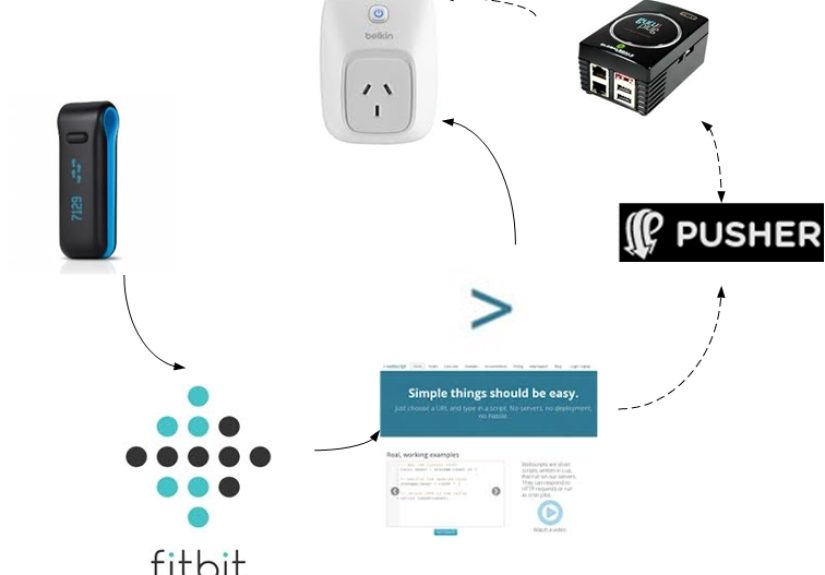
This in-depth article unpacks the bizarre but real DIY story behind the headline 'FitBit Hack Causes Food...
Jill Roth’s story is more than a career profile. It is a sharp lesson in what modern...
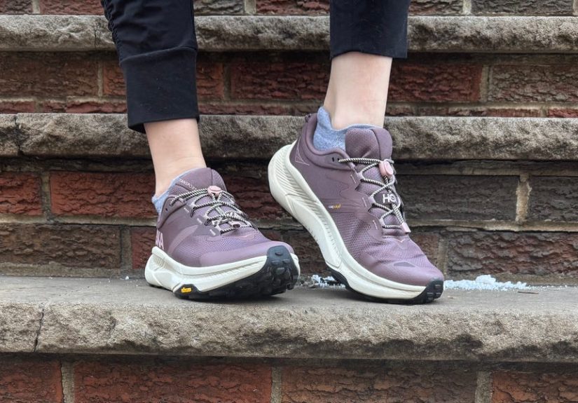
Looking for the best slip-on shoes of 2025? This in-depth guide rounds up 12 standout pairs for...

Marketing teams don’t need more toolsthey need a better system. This in-depth guide breaks down how Asana’s...

The Bella Notte Silk Velvet Quilted Throw Blanket is the kind of luxury home accent that instantly...
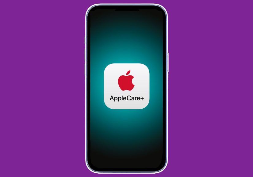
Want to protect your iPhone before life, gravity, or a crowded subway says otherwise? This in-depth guide...

Cocoa butter is famous for soft, glowing skin, but can it really help your face and fade...